
Abstract
Perovskite solar cells (PSCs) have garnered significant attention due to their high power conversion efficiency and simple fabrication process. A challenge in PSC fabrication is forming a uniform, defect-free perovskite layer with long-term operational stability. To address this, antisolvent engineering and surface passivation techniques have been widely adopted. However, commonly used antisolvents such as chlorobenzene and toluene pose significant health and environmental risks due to their toxicity. In this study, tetraethyl orthosilicate (TEOS) was explored as a safer alternative. Devices were fabricated using a carbon-based monolithic structure. Through systematic optimization, using TEOS as an antisolvent yielded a power conversion efficiency (PCE) of 1.16%. Further improvement was achieved by combining TEOS as an antisolvent and a passivation agent, resulting in the highest recorded PCE of 2.28%. These results highlight the potential of TEOS to enhance both the performance and safety profile of PSCs, offering a promising direction for sustainable PSC fabrication.
Keywords: antisolvent, passivation, perovskite solar cell, TEOS
Outline
1. Introduction
The development of solar cell technologies plays a vital role in supporting 7th Sustainable Development Goal, which promotes access to clean and affordable energy1). Among the emerging photovoltaic technologies, perovskite solar cells (PSCs) have shown remarkable progress owing to their rapidly increasing power conversion efficiencies and relatively simple fabrication processes2). Since the pioneering work of Kojima et al.3), continuous improvements have enabled PSCs to approach the performance of conventional photovoltaic technologies4).
A key factor influencing PSC performance is the quality of the perovskite layer5). Poor film quality can introduce defects that promote non-radiative recombination and degrade device performance. Consequently, considerable effort has been devoted to improving perovskite film quality through crystallization engineering and defect management6).
Antisolvent treatment is one of the most widely adopted techniques for promoting rapid crystallization and producing uniform perovskite films7,8). The choice of antisolvent strongly influences crystal growth, grain size, and film morphology9). Another effective approach is surface passivation, which reduces defect density and suppresses charge recombination at grain boundaries and interfaces10). Interface engineering has also been demonstrated to improve charge extraction and operational stability of PSCs11). Furthermore, various passivation materials have been reported to effectively mitigate defect states and improve photovoltaic performance12). The combination of antisolvent treatment and surface passivation, commonly referred to as antisolvent- and surface-assisted crystallization, has become one of the most practical and economical approaches compared with sequential deposition, two‑step deposition, and vapor deposition. Green antisolvent processing has also attracted increasing attention as a sustainable fabrication strategy13).
Traditional antisolvents like chlorobenzene (CB, LD₅₀: 2290 mg·kg⁻¹) and toluene (TL, LD₅₀: 5000 mg·kg⁻¹) are effective but highly toxic. Tetraethyl orthosilicate (TEOS) is introduced as a safer alternative (LD₅₀: 6270 mg·kg⁻¹), offering dual benefits as an antisolvent to enhance crystallization and as a passivation agent to heal surface defects and improve stability14,15). Prior studies have shown the individual success of both TEOS-based passivation and antisolvent methods, highlighting TEOS's potential to combine both advantages efficiently. Isa et al. proposed a passivation method using TEOS by applying small amount of it onto perovskite films in FTO/ TiO2/ CH3NH3PbI3-xClx/ TEOS/ CuSCN/ Carbon PSCs structure16). Meanwhile, Wang et al. introduced TEOS in an antisolvent treatment (ITO/ NiO/ CH3NH3PbI3+TEOS/ PC61BM/ BCP/ Ag), achieving an efficiency of 17.02%14). A similar approach was proposed by Samadpour et al. by incorporating TEOS into chlorobenzene antisolvent for triple cation PSCs17).
However, some of the mentioned studies were developed using a stack architecture that uses a metal counter electrode or processed under controlled environments (i.e., inside a glove box) to suppress the rapid degradation progression of the perovskite material in ambient conditions. To increase the feasibility of PSC on commercialization, further engineering and studies need to be conducted, especially on the fabrication process and device structure. A monolithic electrode structure was proposed to simplify the PSCs structure and remove the dependence on the metal counter electrode by utilizing a carbon counter electrode18,19). Furthermore, PSC processed under ambient conditions needs further research to study the possibility of fabrication outside the glove box to suppress manufacturing costs.
In this study, TEOS was employed simultaneously as both an antisolvent during perovskite film formation and a passivation agent after film deposition. Although TEOS has previously been investigated individually as either an antisolvent or a passivation material for PSCs, its integrated application for both functions in a single fabrication process has received very limited attention. The proposed method could synergistically enhance the structural and electrical quality of the perovskite layer. This approach is especially relevant for monolithic PSC structures, which offer advantages in scalability and fabrication simplicity but typically suffer from lower efficiencies than sandwich- or stack-type architectures. Furthermore, the development of the proposed PSC in ambient conditions provides further insight into the feasibility of a low-manufacturing cost of PSC, in addition to the environmentally safer selection of processing materials. To further evaluate the effectiveness of this strategy, the TEOS concentration was systematically optimized to identify the conditions that provide the best balance between photovoltaic performance, electrical resistance, and long-term stability.
2. Device Configuration
The device structure used in this study was adapted from the architecture reported by previous works, with
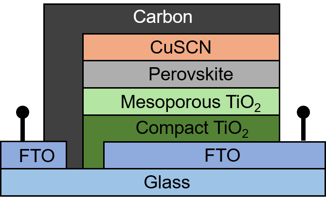
additional investigation focusing on the perovskite layer through the application of antisolvent and passivation methods19). This monolithic configuration supports a simplified fabrication process and offers promising scalability for large-area device production. In this structure, all layers were sequentially deposited onto a fluorine-doped tin oxide (FTO)-coated glass substrate that had been etched to isolate the anode and cathode regions20). Figure 1 shows the layer structure of the monolithic PSC fabricated in this study.
As the electron transport layer (ETL), titanium dioxide (TiO2) was selected due to its transparency and favourable energy alignment with the perovskite. TiO2 has a band gap of approximately 2.8 eV, with conduction and valence band energy levels of −4.1 eV and −7.3 eV, respectively21).
The TiO2 layer was fabricated in two stages using different deposition methods. The compact TiO2 (c-TiO2) was deposited via spray coating to form a dense, pinhole-free layer. The mesoporous TiO2 (m-TiO2) layer was subsequently deposited by spin coating to produce a porous structure22). Such a mesoporous architecture facilitates the infiltration and crystallization of the perovskite absorber within the TiO2 scaffold, thereby increasing the interfacial contact area between the ETL and the active layer23). Improved interfacial contact contributes to more efficient electron extraction and can suppress hysteresis in PSCs24).
The perovskite material used in this study was CH3NH3PbI3-xClx, with a band gap of 1.68 eV, a conduction band minimum at −3.75 eV, and a valence band maximum at −5.43 eV25). These energy levels are well aligned with those of adjacent layers, facilitating efficient charge transport. Copper thiocyanate (CuSCN) was employed as the hole transport layer (HTL) due to its wide band gap of 3.6 eV and favorable energy levels (−1.8 eV conduction, −5.4 eV valence), making it compatible with the perovskite for selective hole extraction26). Graphite-based carbon was used as the top electrode, with a conduction level of approximately
−5.0 eV27), while FTO, which serves as both anode and cathode depending on the charge carrier direction, has a conduction level of −4.4 eV28). A full band diagram
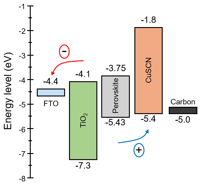
illustrating this device architecture is shown in Figure 2.
3. Experimental Methods
3.1. Materials
The materials used in this study were as follows: FTO glass substrates (sheet resistance: ~7 Ω/sq, Sigma‑Aldrich), titanium (IV) isopropoxide (TTIP, 97%, Sigma-Aldrich), absolute ethanol (EMSURE®, Merck), acetylacetone (ReagenPlus®, Sigma-Aldrich), TiO2 paste (PST-18NR, JCG Catalysts and Chemicals),
methylammonium iodide (MAI, ≥99%, anhydrous, Sigma-Aldrich), lead (II) chloride (PbCl2, 98%, Sigma‑Aldrich), N,N-dimethylformamide (DMF, 99.8%, Sigma-Aldrich), TEOS (98%, reagent grade, Sigma‑Aldrich), CuSCN (99%, Sigma-Aldrich), dipropyl sulphide (DPS, 97%, Sigma-Aldrich), deionized water (Onelab), hydrochloric acid (37%, EMSURE®, Merck), zinc powder (Sigma-Aldrich), and graphite powder (Shanghai Zhanyun Chemical).
The preparation of precursor solutions involved multiple components essential for the fabrication of PSCs. The c-TiO2 precursor was prepared by mixing 0.6 mL TTIP, 0.4 mL acetylacetone, and 9 mL absolute ethanol, stirred at room temperature for 15 minutes to yield a clear yellow solution. For the m-TiO2, a 1:3 mass ratio of TiO2 paste (PST-18NR) to ethanol was stirred for 15 minutes to form a homogeneous white suspension. The perovskite precursor was obtained by dissolving PbCl2 and MAI in anhydrous DMF with a molar ratio of 1:3, then stirred at 80 °C for 1 hour until a deep yellow, precipitate-free solution formed. The CuSCN precursor for the hole transport layer was prepared by dissolving 6 mg/mL of CuSCN powder in DPS, stirred continuously for at least 8 hours at room temperature until a clear and homogeneous solution was achieved. For the electrode, graphite powder was mixed with acetylene black to produce a uniform mixture suitable for use as a carbon electrode.
3.2. Fabrication and Characterization
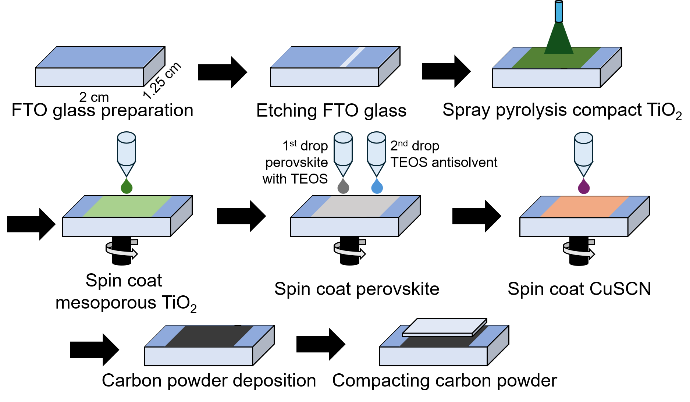
This study comprises fabrication stages and characterization stage, as shown in Figure 3 and all stages were performed under ambient conditions. Substrate preparation involved cutting FTO glass (2.5 cm x 1.25 cm), ultrasonic cleaning in deionized water, ethanol, and acetone (5 min each), and drying at 70 °C. Etching was done using zinc powder and HCl solution (5 min) with Kapton tape masking, followed by rinsing and electrical isolation verification.
The c-TiO2 layer was deposited via spray coating of a 2.5 mL precursor in four layers with intermediate drying at 250 °C and final annealing at 550 °C. The m-TiO2 layer was applied by spin coating (50 µL, 4000 rpm, 20 s) and annealed at 550 °C for 30 min. Perovskite deposition used spin coating (40 µL, 4000 rpm, 20 s) with four variations: pure CH₃NH₃PbI3-xClx, with TEOS passivation, TEOS antisolvent, and a combination. TEOS antisolvent was optimized by drop-casting 0–120 µL (0:1 to 3:1 ratio) 5 s before the spin cycle ended. A further optimization included 0.25 mol% TEOS in the precursor to examine synergy with the antisolvent. CuSCN as the hole transport layer was deposited by spin coating (40 µL, 4000 rpm, 20 s) and annealed at 80 °C for 15 min. The carbon electrode was applied using graphite powder spread and compressed with a glass plate to ensure firm contact with CuSCN. For each experimental condition, three independent devices were fabricated to evaluate the reproducibility of the fabrication process, and the best‑performing device was selected for photovoltaic characterization and discussion.
Device characterization included current-voltage (I-V) measurements in the dark using a Keithley 4200A‑SCS, and under natural sunlight with an irradiance of 700–900 W/m2 around solar noon. The solar irradiance was monitored using a Lutron SPM-1116SD Solar Power Meter (resolution of 0.1 W/m2 for irradiance below 1000 W/m2 and 1 W/m2 for irradiance of 1000 W/m2 or higher), together with a multimeter for electrical measurements. Resistance analysis was performed using electrochemical impedance spectroscopy (EIS) (0.1 Hz – 200 kHz) with a PalmSens EmStat4s.
Table 1: Measured photovoltaic parameters of TEOS antisolvent only optimization
| Drop Volume (µL) | VOC (V) | JSC (mA/cm2) | FF | PCE (%) |
|---|---|---|---|---|
| 0 | 0.69 | 0.28 | 0.53 | 0.34 |
| 40 | 1.15 | 0.34 | 0.71 | 0.90 |
| 80 | 0.93 | 0.52 | 0.69 | 1.06 |
| 120 | 0.83 | 0.15 | 0.79 | 0.30 |
4. Results and Discussion
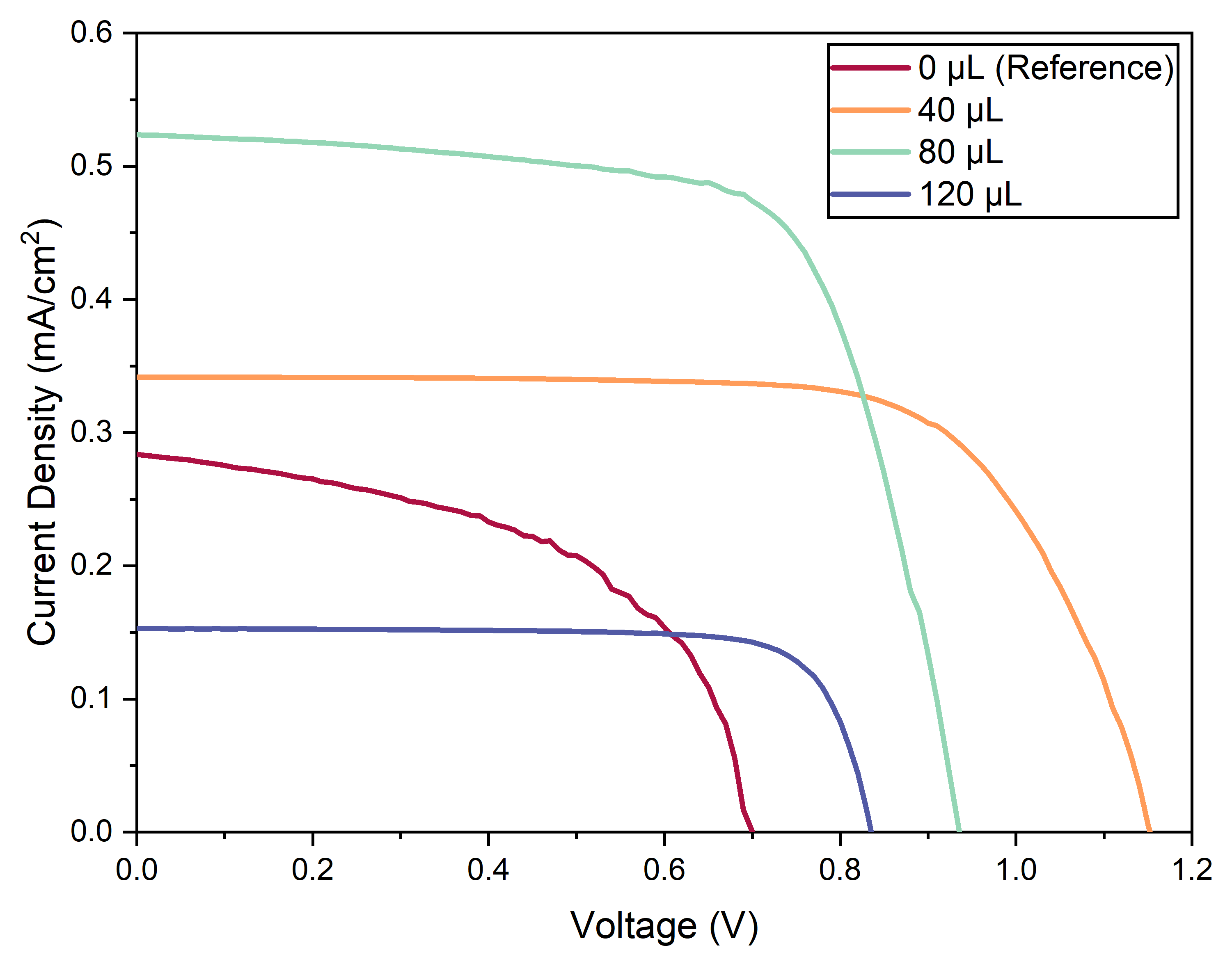
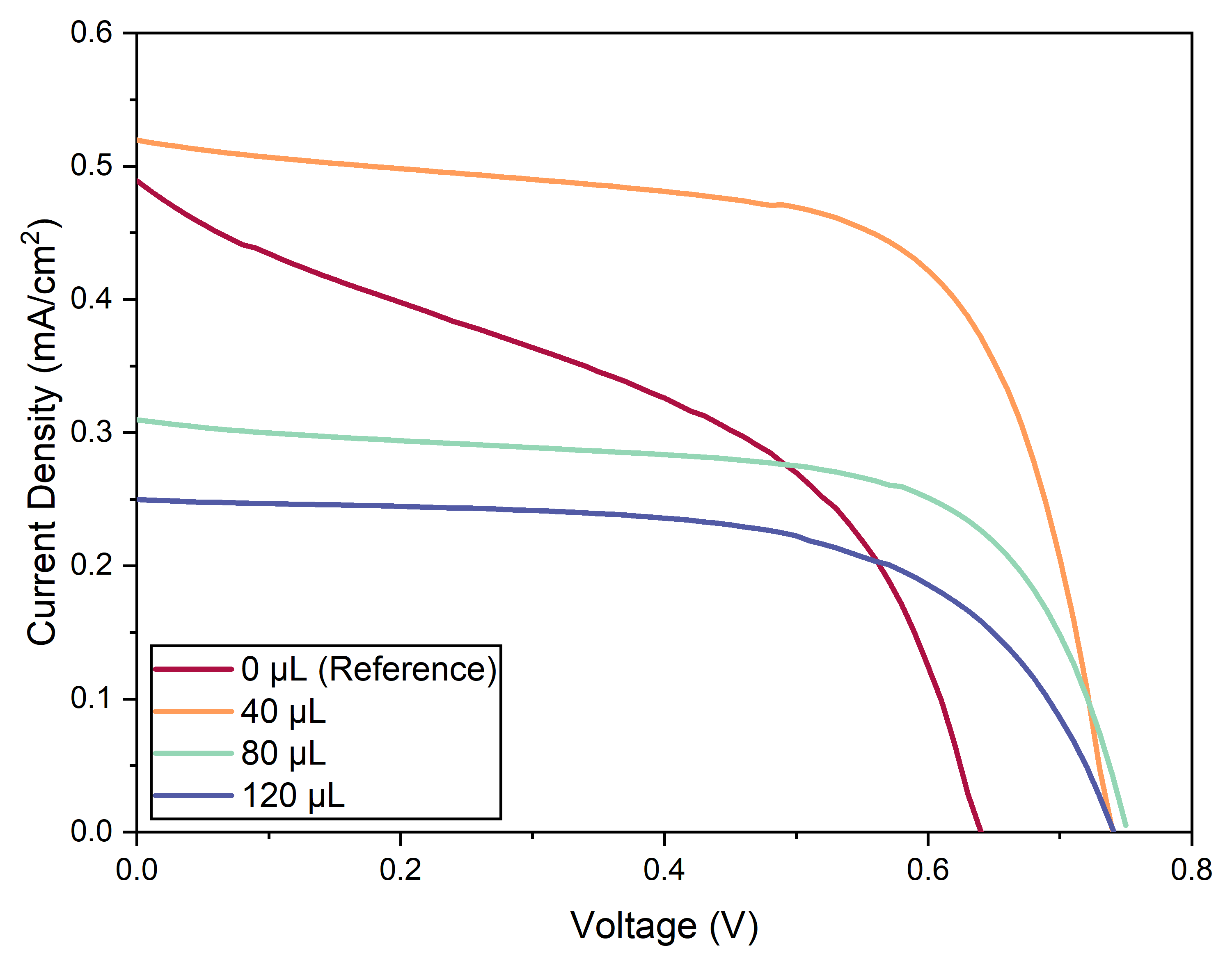
The photovoltaic performance shown in Table 1 derived from the current density-voltage (J-V) curve (Figure 4) is the result of an optimization study using TEOS as an antisolvent only, without any additional passivation treatment. Among the tested drop volumes, the optimal amount of TEOS was found to be 80 µL, yielding the highest power conversion efficiency (PCE) of 1.06%.This performance improvement is mainly due to the significant increase in short-circuit current density (JSC), which reached 0.52 mA/cm² at 80 µL. Although the fill factor (FF) and open-circuit voltage (VOC) remained relatively stable or even improved at higher drop volumes (e.g., 120 µL), the sharp decrease in JSC resulted in a notable drop in efficiency (down to 0.30%). It was observed that varying the volume of TEOS as an antisolvent significantly impacts the crystallization and efficiency of PSCs. It worth noting that insufficient antisolvent slows crystallization whereas excessive antisolvent causes rapid crystallization and material loss29).
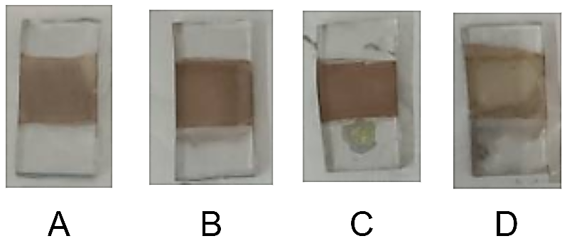
In addition to electrical measurements, Figure 5 shows the macroscopic appearance of the perovskite films with different TEOS drop volumes. Among all samples, the film treated with 80 µL of TEOS appears the most uniform and homogeneous, suggesting better film formation. This improved surface quality likely contributes to the higher photovoltaic performance observed in the optimized condition.
Subsequent optimization of the TEOS drop volume in the combined antisolvent–passivation strategy (with
0.25 mol% TEOS as passivation additive) revealed that a drop volume of 40 µL yielded the best photovoltaic performance. Conversely, the lowest efficiency was obtained from the sample with a 120 µL drop volume. This combined method resulted in a 74.8% increase in efficiency compared to the sample using only the passivation method (0 µL drop volume). Notably, the optimal range of drop volumes in the combined method is narrower than in the antisolvent-only optimization, which showed optimal performance at both 40 µL and 80 µL. In contrast, the combined method showed a clear efficiency peak exclusively at 40 µL, as illustrated in Figure 6 (with corresponding photovoltaic performance in Table 2).
The reduction in the optimal drop volume suggests an interaction between TEOS introduced during the passivation step and the antisolvent, which likely arises from enhanced supersaturation induced by TEOS in the precursor. Under ambient conditions, TEOS hydrolyses into silanol and ethanol, as shown in Equation 1.
The silanol increases the solute concentration in the precursor solution, promoting an earlier onset of supersaturation30). As a result, a lower amount of antisolvent is needed to reach the optimal crystallization point. This explains why 40 µL was optimal in the combined method, compared to 80 µL in the antisolvent‑only condition.
Macroscopic inspection of the perovskite layers, shown in Figure 7, indicates no drastic visual difference between most samples. However, the perovskite layer under 40 µL conditions, displayed the darkest and most uniform
Table 2: Photovoltaic parameters of PSCs with perovskite passivation, processed using different TEOS antisolvent volumes
| Drop Volume (µL) | VOC (V) | JSC (mA/cm2) | FF | PCE (%) |
|---|---|---|---|---|
| 0 | 0.63 | 0.49 | 0.44 | 0.66 |
| 40 | 0.73 | 0.52 | 0.67 | 1.16 |
| 80 | 0.75 | 0.31 | 0.65 | 0.69 |
| 120 | 0.74 | 0.25 | 0.62 | 0.48 |
perovskite film, indicating the best crystallization quality among the tested conditions. In contrast, the 120 µL sample showed visible inhomogeneity due to excessive antisolvent, while the 0 µL sample appeared pale, indicating insufficient crystal growth.
Finally, Table 3 presents the results of the photovoltaic performance parameters measured for four different samples: reference (without treatment), antisolvent, passivation, and the combination of antisolvent and passivation. Figure 8 shows the J-V curves for each sample. The combination sample shows the highest PCE at 2.28%, followed by the passivation sample (1.82%), antisolvent (1.28%), and the reference sample (0.61%). The highest JSC is found in the combination sample (3.12 mA/cm²), while the VOC remains relatively consistent across the three samples with methods, ranging between 0.80–0.82 V. The reference sample exhibits the lowest values for both VOC and JSC.
The efficiency improvement can be attributed to two enhancement mechanisms: first, the passivation method plays a role in minimizing pinholes through the formation of a SiO2 structure; second, the antisolvent method promotes the growth of perovskite crystals with improved uniformity and morphology31,32).
Figure 9 presents the efficiency measurements after 7 and 14 days of storage at room temperature and 50–70% humidity. The combination sample (antisolvent and passivation) shows the best performance in maintaining its efficiency, with only a slight decrease of 2.3% after 14 days. In contrast, the reference sample experiences a efficiency drop, with a 42.5% decrease after 14 days, indicating a much higher instability under these conditions. Previous research indicates that TEOS-based passivation also forms a SiO2 layer that acts as a barrier against moisture, which would otherwise degrade the perovskite layer32,33). Furthermore, Samadpour et al, highlighted that perovskite films with poor homogeneity and numerous pinholes are more susceptible to degradation due to increased pore density, which allows for greater exposure
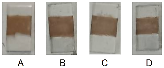
Table 3: Photovoltaic performance parameters of PSCs under different antisolvent and passivation treatments
| Condition | VOC (V) | JSC (mA/cm2) | FF | PCE (%) |
|---|---|---|---|---|
| Reference | 0.61 | 0.10 | 0.65 | 0.61 |
| Antisolvent | 0.80 | 1.29 | 0.71 | 1.28 |
| Passivation | 0.82 | 2.35 | 0.64 | 1.82 |
| Antisolvent + Passivation | 0.82 | 3.12 | 0.63 | 2.28 |
to moisture and a higher likelihood of ion diffusion17).
Impedance analysis using Nyquist plots in Figure 10 and the corresponding resistance values (Table 4) reveal significant variation in the recombination resistance (Rrec) among the samples, with the combination sample showing the highest Rrec value of 3868.5 Ω, indicating the lowest recombination rate. In contrast, the reference sample has the lowest Rrec at 535.62 Ω, reflecting a higher recombination rate34).
The series resistance (Rseries) and charge transfer resistance (Rtrans) remain relatively similar across all samples, showing no significant variation.
The relatively constant Rseries values in this study arise from the similar electrode configuration and the PSCs’ structure across the samples. It is worth noting that the Rseries value depends on the conductivities of the electrodes (FTO and carbon) as well as the bulk resistance of the devices35).
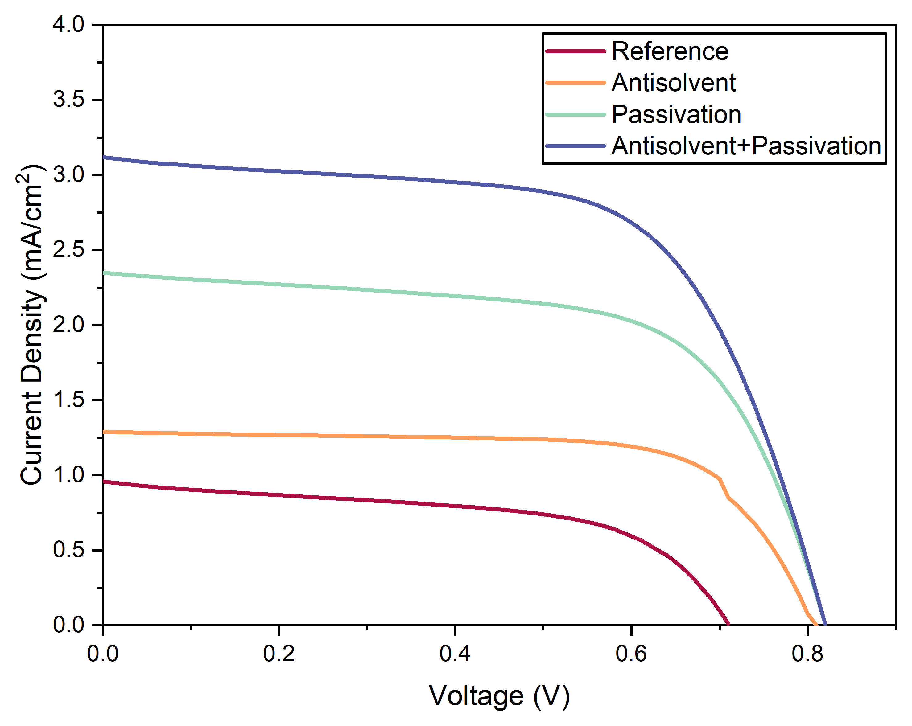
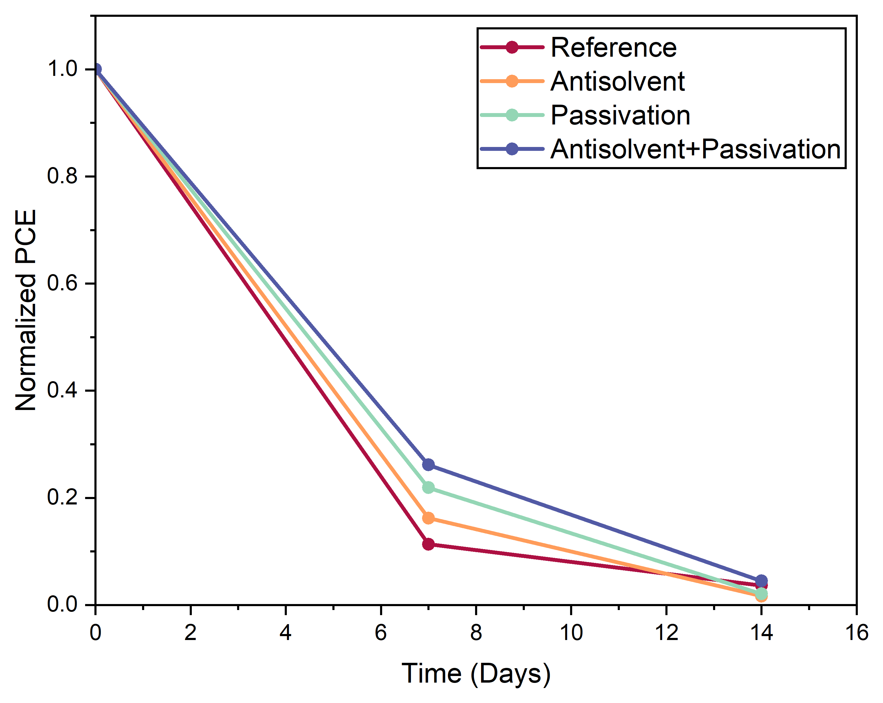
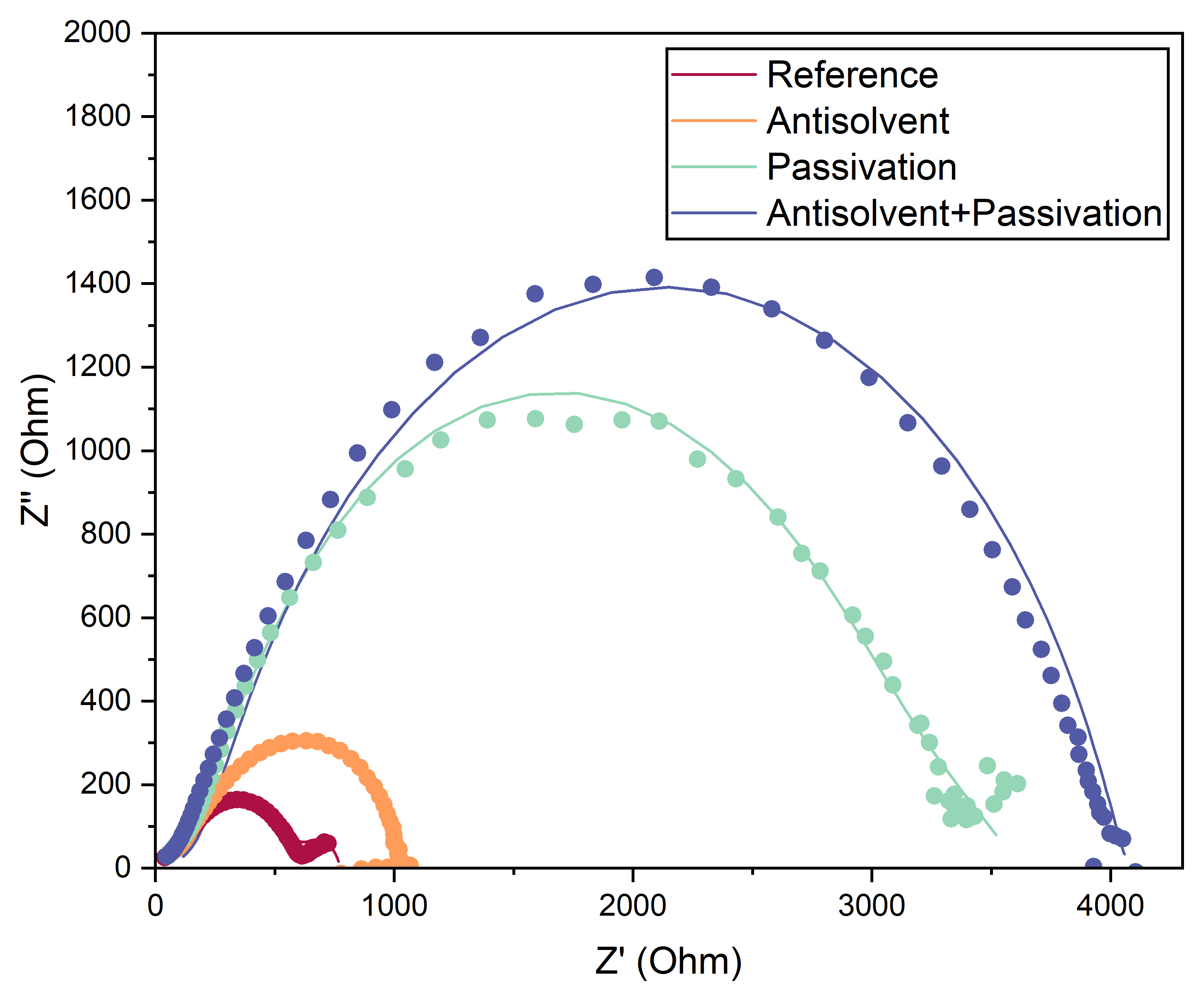
Table 4: Resistance value derived from EIS measurement
| Condition | Rseries (Ω) | Rtrans (Ω) | Rrec (Ω) |
|---|---|---|---|
| Reference | 24.31 | 102.65 | 535.62 |
| Antisolvent | 30.31 | 102.60 | 889.36 |
| Passivation | 25.95 | 121.68 | 325.60 |
| Antisolvent + Passivation | 25.87 | 118.63 | 3868.50 |
On the other hand, variations in Rtrans may arise from differences in interfacial charge-transfer resistance; however, because no variation in interfacial layers was introduced among the tested samples, it can be inferred that the interfacial properties across all samples are uniform. The impedance measurement aligns with photovoltaic performance: the combination sample, which has the highest Rrec, has the highest efficiency, whereas the reference sample, with the lowest Rrec, exhibits the lowest efficiency.
Previous studies have reported that improved perovskite crystallization and effective defect passivation suppress non-radiative recombination, resulting in higher recombination resistance and enhanced photovoltaic performance35). Therefore, the correlation between the photovoltaic performance and impedance characteristics observed in this study is consistent with the proposed role of the combined TEOS antisolvent and passivation treatment in improving the quality of the perovskite layer. Nevertheless, direct morphological and structural characterization will be required to further verify this mechanism in future work.
Although the highest PCE achieved in this study was relatively modest, the results can be interpreted in the context of the device architecture and fabrication conditions. The use of a monolithic carbon-based structure generally results in lower efficiencies than conventional sandwich-type PSCs because of less efficient charge extraction and higher interfacial resistance associated with carbon electrodes18). In addition, device fabrication under ambient conditions exposes the perovskite layer to moisture, which can accelerate degradation during processing and affect film quality and photovoltaic performance36). Nevertheless, the use of TEOS as a low‑toxicity antisolvent and passivation agent, together with ambient processing and monolithic carbon‑based electrodes, demonstrates a promising approach toward environmentally safer and scalable PSC fabrication. Further improvements in interface engineering, film quality, and environmental control during fabrication are expected to enhance device performance.
5. Conclusions
To sum this up, the combination of 40 µL TEOS as an antisolvent and 0.25 mol% TEOS for passivation in CH3NH3PbI3-xClx perovskite fabrication proved to be the most effective approach, resulting in the highest efficiency of 2.28% and enhanced device stability. This method notably increased the Rrec to 3868.5 Ω while keeping Rseries and Rtrans relatively consistent, thereby confirming its role in suppressing secondary recombination and improving the structural and electrical quality of the perovskite layer.
CRediT Authorship Contribution
Muhammad Akmal Prabowo: Conceptualization, Methodology, Investigation, Formal analysis, Visualization, and Writing – Original Draft. Junivan Sulistianto: Writing - Review & Editing, Validation, Visualization. Nji Raden Poespawati: Funding acquisition, Supervision, Project administration.
Declaration of Competing Interest
The authors have no competing interests to declare that are relevant to the content of this article.
Data Availability
Data will be made available on request.
Acknowledgements
The authors acknowledge the financial support provided by the Faculty of Engineering, Universitas Indonesia, through the Professor, Associate Professor, and Senior Lecturer Research Grant Scheme (Fiscal Year 2024/2025, Contract No. NKB-3448/UN2.F4.D/PPM.00.00/2024). The authors also would like to express their sincere gratitude to Nano Device Laboratory Prof. Dr. Ir. Djoko Hartanto, M.Sc., for providing research facilities and support.
References
- International Energy Agency, “Net zero by 2050: a roadmap for the global energy sector,” Int. Energy Agency, 224 (2021). https://www.iea.org/reports/net-zero-by-2050.
- R.A. Afre, and D. Pugliese, “Perovskite solar cells: a review of the latest advances in materials, fabrication techniques, and stability enhancement strategies,” Micromachines, 15 (2) 192 (2024). doi:10.3390/mi15020192.
- A. Kojima, K. Teshima, Y. Shirai, and T. Miyasaka, “Organometal halide perovskites as visible- light sensitizers for photovoltaic cells,” J Am Chem Soc, 131 (October) 6050–6051 (2009). doi:10.1021/ja809598r.
- M.K. Assadi, S. Bakhoda, R. Saidur, and H. Hanaei, “Recent progress in perovskite solar cells,” Renew. Sustain. Energy Rev., 81 (October 2016) 2812–2822 (2018). doi:10.1016/j.rser.2017.06.088.
- T. Seyisi, B.G. Fouda-Mbanga, J.I. Mnyango, Y.B. Nthwane, B. Nyoni, S. Mhlanga, S.P. Hlangothi, and Z. Tywabi-Ngeva, “Major challenges for commercialization of perovskite solar cells: a critical review,” Energy Reports, 13 1400–1415 (2025). doi:10.1016/j.egyr.2025.01.019.
- J. Yang, S. Chen, J. Xu, Q. Zhang, H. Liu, Z. Liu, and M. Yuan, “A review on improving the quality of perovskite films in perovskite solar cells via the weak forces induced by additives,” Appl. Sci., 9 (20) 4393 (2019). doi:10.3390/app9204393.
- D. Gedamu, I.M. Asuo, D. Benetti, M. Basti, I. Ka, S.G. Cloutier, F. Rosei, and R. Nechache, “Solvent-antisolvent ambient processed large grain size perovskite thin films for high-performance solar cells,” Sci. Rep., 8 (1) 1–11 (2018). doi:10.1038/s41598-018-31184-0.
- I.M. Asuo, D. Gedamu, N.Y. Doumon, I. Ka, A. Pignolet, S.G. Cloutier, and R. Nechache, “Ambient condition-processing strategy for improved air-stability and efficiency in mixed-cation perovskite solar cells,” Mater. Adv., 1 (6) 1866–1876 (2020). doi:10.1039/d0ma00528b.
- A.D. Taylor, Q. Sun, K.P. Goetz, Q. An, T. Schramm, Y. Hofstetter, M. Litterst, F. Paulus, and Y. Vaynzof, “A general approach to high-efficiency perovskite solar cells by any antisolvent,” Nat. Commun., 12 (1) 1878 (2021). doi:10.1038/s41467-021-22049-8.
- Q. Jiang, Y. Zhao, X. Zhang, X. Yang, Y. Chen, Z. Chu, Q. Ye, X. Li, Z. Yin, and J. You, “Surface passivation of perovskite film for efficient solar cells,” Nat. Photonics, 13 (7) 460–466 (2019). doi:10.1038/s41566-019-0398-2.
- C. Zhao, H. Zhang, A. Krishna, J. Xu, and J. Yao, “Interface engineering for highly efficient and stable perovskite solar cells,” Adv. Opt. Mater., 12 (7) (2024). doi:10.1002/adom.202301949.
- X. Zheng, B. Chen, J. Dai, Y. Fang, Y. Bai, Y. Lin, H. Wei, X.C. Zeng, and J. Huang, “Defect passivation in hybrid perovskite solar cells using quaternary ammonium halide anions and cations,” Nat. Energy, 2 (7) 17102 (2017). doi:10.1038/nenergy.2017.102.
- M. Zhang, Z. Wang, B. Zhou, X. Jia, Q. Ma, N. Yuan, X. Zheng, J. Ding, and W. Zhang, “Green anti‐solvent processed planar perovskite solar cells with efficiency beyond 19%,” Sol. RRL, 2 (2) (2018). doi:10.1002/solr.201700213.
- M. Wang, Q. Fu, L. Yan, P. Guo, L. Zhou, G. Wang, Z. Zheng, and W. Luo, “Improving the performance and reproducibility of inverted planar perovskite solar cells using tetraethyl orthosilicate as the antisolvent,” ACS Appl. Mater. Interfaces, 11 (4) 3909–3916 (2019). doi:10.1021/acsami.8b18402.
- H.J. Kim, Y.J. Kim, G.S. Han, and H.S. Jung, “Green solvent strategies toward sustainable perovskite solar cell fabrication,” Sol. RRL, 8 (5) (2024). doi:10.1002/solr.202300910.
- M.J. Abraham Isa, N. Raden Poespawati, C.M. Alma, L. Kevin, R. Rembianov, and J. Sulistianto, “Employing Tetra-ethyl Orthosilicate (TEOS) Concentration to Optimize Perovskite Solar Cell Performance,” in: 2020 12th Int. Conf. Inf. Technol. Electr. Eng., IEEE, 2020: pp. 80–85. doi:10.1109/ICITEE49829.2020.9271754.
- M. Samadpour, A. Golchini, K. Abdizadeh, M. Heydari, M. Forouzandeh, Z. Saki, and N. Taghavinia, “Modified antisolvent method for improving the performance and stability of triple-cation perovskite solar cells,” ACS Omega, 6 (1) 172–179 (2021). doi:10.1021/acsomega.0c04058.
- J. Sulistianto, A. Konno, N.R. Poespawati, and T. Abuzairi, “Acetylene black as counter electrode on monolithic perovskite solar cell,” Proc. Int. Conf. Electr. Eng. Informatics, 2022-Octob 42–46 (2022). doi:10.1109/IConEEI55709.2022.9972311.
- J. Sulistianto, A. Konno, T. Abuzairi, and N.R. Poespawati, “Perovskite solar cells with modified carbon electrode and cuscn interlayer processed under ambient conditions,” Int. J. Photoenergy, 2024 (1) (2024). doi:10.1155/2024/5355903.
- A.E. Shalan, “Challenges and approaches towards upscaling the assembly of hybrid perovskite solar cells,” Mater. Adv., 1 (3) 292–309 (2020). doi:10.1039/D0MA00128G.
- H. Wang, X. Hu, and H. Chen, “The effect of carbon black in carbon counter electrode for CH3NH3PbI3/TiO2 heterojunction solar cells,” RSC Adv., 5 (38) 30192–30196 (2015). doi:10.1039/C5RA02325D.
- X.-H. Zhang, J.-J. Ye, L.-Z. Zhu, H.-Y. Zheng, X.-P. Liu, X. Pan, and S.-Y. Dai, “High consistency perovskite solar cell with a consecutive compact and mesoporous tio 2 film by one-step spin-coating,” ACS Appl. Mater. Interfaces, 8 (51) 35440–35446 (2016). doi:10.1021/acsami.6b11860.
- A. Hernández-Granados, A.N. Corpus-Mendoza, P.M. Moreno-Romero, C.A. Rodríguez-Castañeda, J.E. Pascoe-Sussoni, O.A. Castelo-González, E.C. Menchaca-Campos, J. Escorcia-García, and H. Hu, “Optically uniform thin films of mesoporous TiO2 for perovskite solar cell applications,” Opt. Mater. (Amst)., 88 (December 2018) 695–703 (2019). doi:10.1016/j.optmat.2018.12.044.
- Y. Rong, Y. Hu, S. Ravishankar, H. Liu, X. Hou, Y. Sheng, A. Mei, Q. Wang, D. Li, M. Xu, J. Bisquert, and H. Han, “Tunable hysteresis effect for perovskite solar cells,” Energy Environ. Sci., 10 (11) 2383–2391 (2017). doi:10.1039/C7EE02048A.
- S.A. Bretschneider, J. Weickert, J.A. Dorman, and L. Schmidt-Mende, “Research update: physical and electrical characteristics of lead halide perovskites for solar cell applications,” APL Mater., 2 (4) (2014). doi:10.1063/1.4871795.
- J.W. Jung, C.C. Chueh, and A.K.Y.K. ‐Y. Jen, “High‐Performance semitransparent perovskite solar cells with 10% power conversion efficiency and 25% average visible transmittance based on transparent cuscn as the hole‐transporting material,” Adv. Energy Mater., 5 (17) 1–7 (2015). doi:10.1002/aenm.201500486.
- Z. Ku, Y. Rong, M. Xu, T. Liu, and H. Han, “Full printable processed mesoscopic CH3NH3PbI3/TiO2 heterojunction solar cells with carbon counter electrode,” Sci. Rep., 3 (2013). doi:10.1038/srep03132.
- Q. Qiao, J. Beck, R. Lumpkin, J. Pretko, and J.T. Mcleskey, “A comparison of fluorine tin oxide and indium tin oxide as the transparent electrode for P3OT/TiO2 solar cells,” Sol. Energy Mater. Sol. Cells, 90 (7–8) 1034–1040 (2006). doi:10.1016/j.solmat.2005.05.020.
- K.-M.M. Lee, C.-J.J. Lin, B.-Y.Y. Liou, S.-M.M. Yu, C.-C.C. Hsu, V. Suryanarayanan, and M.-C.C. Wu, “Selection of anti-solvent and optimization of dropping volume for the preparation of large area sub-module perovskite solar cells,” Sol. Energy Mater. Sol. Cells, 172 (May) 368–375 (2017). doi:10.1016/j.solmat.2017.08.010.
- B.A. De Carvalho, S. Kavadiya, S. Huang, D.M. Niedzwiedzki, and P. Biswas, “Highly stable perovskite solar cells fabricated under humid ambient conditions,” IEEE J. Photovoltaics, 7 (2) 532–538 (2017). doi:10.1109/JPHOTOV.2016.2642639.
- Z. Wang, H. Gao, D. Wu, J. Meng, J. Deng, and M. Cui, “Defects and defect passivation in perovskite solar cells,” Molecules, 29 (9) 2104 (2024). doi:10.3390/molecules29092104.
- M. Guan, Q. Zhang, F. Wang, H. Liu, J. Zhao, C. Jia, Y. Chen, M. Guan, Q. Zhang, Y. Chen, F. Wang, H. Liu, and J. Zhao, “Employing tetraethyl orthosilicate additive to enhance trap passivation of planar perovskite solar cells,” Electrochim. Acta, 293 174–183 (2019). doi:10.1016/j.electacta.2018.10.043.
- H. Lei, P. Dai, X. Wang, Z. Pan, Y. Guo, H. Shen, J. Chen, J. Xie, B. Zhang, S. Zhang, and Z. Tan, “In situ defect passivation with silica oligomer for enhanced performance and stability of perovskite solar cells,” Adv. Mater. Interfaces, 7 (3) (2020). doi:10.1002/admi.201901716.
- P.F. Betancur, O.E. Solis, R. Abargues, T.S. Ripolles, and P.P. Boix, “Recombination resistance identification through current–voltage curve reconstruction in perovskite solar cells,” Phys. Chem. Chem. Phys., 26 (48) 29904–29912 (2024). doi:10.1039/D4CP04143G.
- A. Guerrero, J. Bisquert, and G. Garcia-Belmonte, “Impedance spectroscopy of metal halide perovskite solar cells from the perspective of equivalent circuits,” Chem. Rev., 121 (23) 14430–14484 (2021). doi:10.1021/acs.chemrev.1c00214.
- N.K. Kim, Y.H. Min, S. Noh, E. Cho, G. Jeong, M. Joo, S.W. Ahn, J.S. Lee, S. Kim, K. Ihm, H. Ahn, Y. Kang, H.S. Lee, and D. Kim, “Investigation of thermally induced degradation in CH3NH3PbI3 perovskite solar cells using in-situ synchrotron radiation analysis,” Sci. Rep., 7 (1) 1–9 (2017). doi:10.1038/s41598-017-04690-w.